Every PCB has a power distribution network, and every power distribution network has an opinion about your design. Copper that looked generous in the layout editor turns out to drop 60 mV by the time it reaches the furthest IC. A via cluster that seemed like overkill is quietly running near its current limit. None of this is visible in the schematic, and most of it is invisible in the layout too — until you measure it on a fabricated board, or simulate it before you get there.
This article explains what a PDN is and why its DC behavior matters, then introduces PDN Analyzer by Elecmore v1.1, our free Public Beta tool that brings PCB power integrity analysis directly into a KiCad workflow. If you already know why you need PDN analysis, you can skip straight to the PDN Analyzer download page — it is free during the Public Beta for Windows 10 and Windows 11.
Free Public Beta
PDN Analyzer v1.1 for Windows 10 & Windows 11
What Is a PCB PDN?
The power distribution network (PDN) is everything that carries power from your supply or regulator output to the power pins of every component on the board: copper pours and planes, traces, neck-downs, vias, connector pins and the return path back through ground. Power distribution network analysis is the discipline of checking that this whole path actually delivers the voltage and current each load expects.
It is easy to think of a 5 V rail as “5 volts everywhere”. Physically, it is not. Copper has resistance — roughly 0.5 mΩ per square for 1 oz foil — and every amp that flows through that resistance converts into a voltage difference across the copper. The PDN is therefore a distributed resistor network, and each IC sits at a slightly different voltage depending on where it is, how much current it draws, and what else is drawing current along the same copper.
Why Voltage Drop and Current Density Matter
Voltage drop (IR drop)
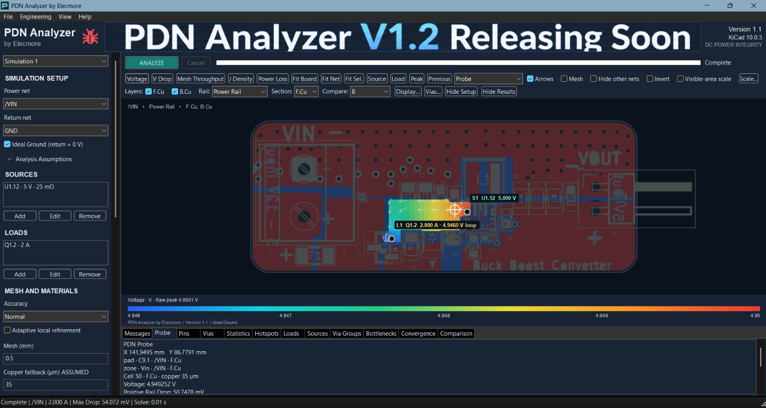
Digital and analog ICs specify a supply tolerance — commonly ±5% or ±3% on a rail. That tolerance budget is shared between regulator accuracy, ripple, transient response and the DC drop across the PDN. If your regulator is within 1% and ripple is 20 mV, but the copper drops 54 mV to the furthest load (a real number from the board shown later in this article), you may have silently consumed most of the margin before the design even reaches bring-up. PCB voltage drop analysis tells you the actual rail voltage at each load, on the real geometry, instead of a hand-waved estimate.
Current density
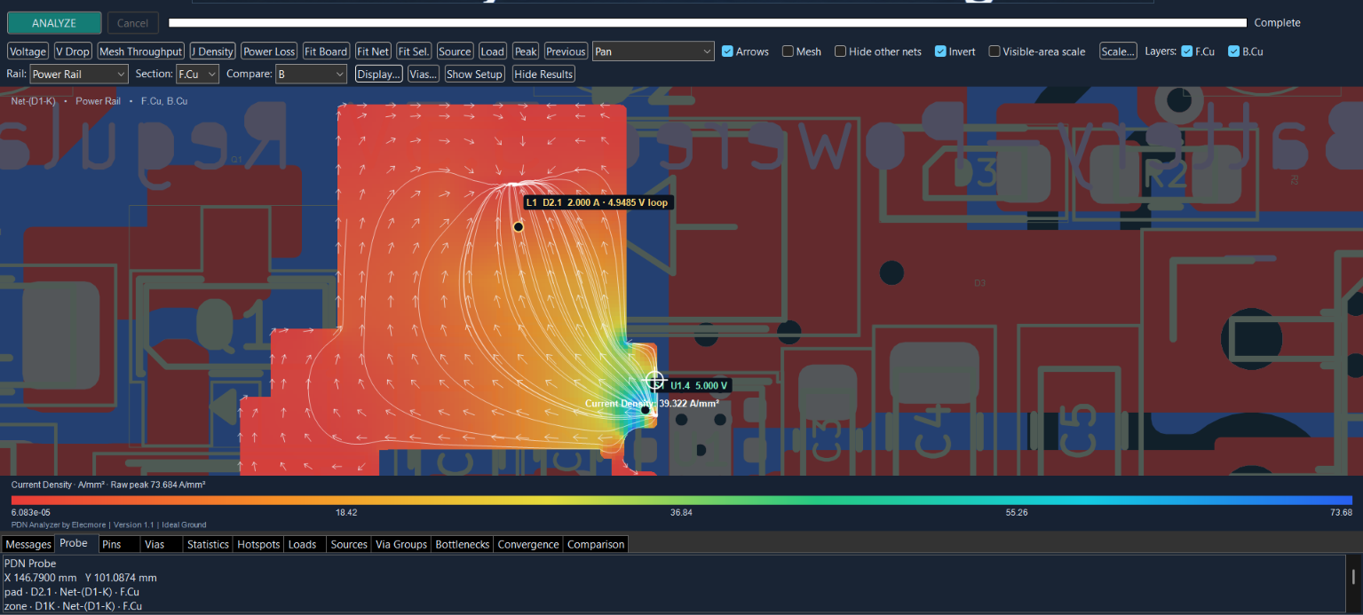
Current does not spread itself evenly. It crowds into the narrowest part of the path: a neck-down between a connector and a plane, the copper bridge between two via clusters, the thin web of plane left between antipad clearances. High current density means local I²R heating, and in extreme cases long-term reliability concerns in the copper itself. PCB current density analysis shows where the current is concentrating, measured in A/mm², so you can widen the copper or add parallel paths where it actually matters. On the example board below, current density peaks at 73.7 A/mm² — exactly the kind of hotspot that is invisible until you solve for it.
Power loss
Every milliohm carrying amps dissipates power as heat: P = I²R. A few hundred milliwatts spread across a plane is usually harmless; the same loss concentrated in a short neck-down or a single via creates a local hot spot right where you cannot heatsink it. Locating the worst power-loss regions during layout is far cheaper than finding them with a thermal camera during validation.
Return-path and ground behavior
Current loops are completed through the return path, and the return is not an ideal zero-ohm ground. Return current crowds under the forward path and through the nearest vias, and the resulting voltage gradient across the ground plane means “ground” is at a slightly different potential at different points on the board. Shared returns couple circuits together: a noisy load’s return current modulates the ground reference of everything sharing that stretch of copper. Analyzing the finite return network — rather than assuming an ideal ground — is what separates real PDN analysis from a resistance calculator.
PCB bottlenecks and via current
The most common PDN failures are geometric: a wide plane that funnels through a narrow corridor, or a high-current rail that crosses layers through too few vias. A single via carries a finite amount of current comfortably, and paralleling vias only helps if the copper feeding them is wide enough. These bottlenecks are hard to spot by eye in a dense layout — especially under BGAs and around connector fields — but they stand out immediately in a current-density overlay.
Why analyze before fabrication?
Because the cost curve is brutal. A PDN fix in the layout editor costs minutes: widen a pour, add vias, move a load. The same fix after fabrication costs a board respin — weeks of calendar time and real money — or worse, an awkward bodge on a “finished” product. DC PDN simulation at the layout stage turns power integrity from a post-mortem activity into a design step.
PDN Analysis in KiCad
KiCad is an excellent schematic and layout environment — it is what we use for much of our own work at Elecmore — but it does not include a built-in DC power integrity solver. The traditional options are estimating drops with spreadsheets and copper-resistance rules of thumb, exporting geometry into a general-purpose field solver, or buying into a high-cost ECAD suite with an integrated PI module. For a large share of KiCad PCB analysis work, none of these are a good fit: estimates miss the actual geometry, and full PI suites are priced for enterprise teams.
That gap is exactly why we built PDN Analyzer: a focused desktop tool that does DC PDN simulation on the board you are actually editing, launched from inside the KiCad PCB Editor, with results overlaid on the layout you already understand.
PDN Analyzer by Elecmore
PDN Analyzer by Elecmore is a Windows application that runs as an external plugin for the KiCad 10 PCB Editor. The workflow is deliberately short:
- Open your PCB in KiCad — open the board in the KiCad 10 PCB Editor as usual.
- Launch the plugin — Tools → External Plugins → PDN Analyzer by Elecmore.
- Analyze and inspect — define sources and loads, run the analysis and inspect the results overlaid on the board.
Version 1.1 meshes the real copper geometry of the selected nets, solves the steady-state DC problem, and presents the results where they happen. The feature set:
- Voltage analysis — rail voltage mapped across the real copper geometry.
- Voltage drop — see exactly where resistance is costing you rail margin, and how much.
- Current density — current concentration through traces, neck-downs, vias and planes, in A/mm².
- Power loss — locate the regions dissipating the most power.
- Return path analysis — finite ground/return behavior instead of an ideal-ground assumption.
- PCB visualization — engineering results overlaid directly on the board geometry.
- Probe & locate peak — click any point to read its value, or jump straight to the worst-case location.
- Reports & exports — reports, CSV and PNG exports for design reviews and documentation.
Your design data stays on your computer: the analysis runs locally, optional diagnostics are off by default, and nothing about your PCB leaves the machine. Details are in the PDN Analyzer privacy policy.
Real PCB Visualization
This is what PCB power distribution analysis looks like on an actual board. The voltage overlay below maps the rail across the copper; probing the furthest point of this network reads 4.949252 V against the 5 V source — a 54.072 mV worst-case drop, solved in hundredths of a second.
The current-density view answers the other half of the question: where is the copper working hardest? Here the J-density overlay peaks at 73.684 A/mm², flagging a constriction worth widening before release.
And here is the full workflow — from opening the board in KiCad to reading the overlays:
Windows 10 and Windows 11 Downloads
PDN Analyzer v1.1 is free during the Public Beta, with separate builds for each supported platform:
- Windows 11 — PDN Analyzer v1.1 for Windows 11, tested on Windows 11 x64 with KiCad 10.0.6 x64.
- Windows 10 — PDN Analyzer v1.1 for Windows 10, tested on Windows 10 x64 with KiCad 10.0.6 x64, available as an installer or a complete ZIP.
Both downloads, the release notes, the installation guide and the SHA-256 checksums for verifying your download are on the PDN Analyzer download page. The installers are not yet Authenticode-signed, so do verify the SHA-256 of whatever you download against the value published there.
v1.1.0 Public Beta · Free
Download PDN Analyzer for Windows 10 or 11
Who Is It For?
Anyone doing PCB design in KiCad who cares about getting power right the first time: independent hardware designers and consultants who cannot justify enterprise PI tooling, startups iterating quickly on boards, engineering students learning what a PDN actually does, and professional teams who want a fast DC sanity check inside the layout flow before committing to fabrication. If your board carries more than an amp or two, or your rails have tight tolerances, DC power integrity analysis belongs in your checklist — and now it costs nothing to add it.
Professional PCB & Power Integrity Engineering
PDN Analyzer grew out of the work we do every day at Elecmore. We are a hardware engineering studio specialising in high-speed PCB design and full product development: custom motherboard design, SoM carrier boards, DDR3/DDR4/DDR5 memory interfaces, PCIe, USB high-speed interfaces and Ethernet, RF PCB design, and the power integrity and signal integrity work that holds all of it together — PDN review, schematic review and PCB layout review included. We also take designs further into embedded hardware development when a project needs it. If any of that sounds like the problem on your desk, our engineering services page has the details.
Feedback and Future Development
v1.1 is a Public Beta, and the roadmap is being shaped by the people using it. Inside PDN Analyzer, click the red bug icon and choose what you want to send:
- Bug Report — something is wrong; tell us what happened and what you expected.
- Feature Request — the analysis or workflow you wish it had.
- Feedback — general impressions, usability, documentation.
- Help / Question — you are stuck or unsure how to get a result.
Feedback goes directly to the Elecmore engineering team — the same people who built the solver. Optional diagnostics start unchecked, and your PCB data never leaves your computer unless you explicitly choose to share something with us.
Work With Us
Need help with a high-speed PCB, custom motherboard, SoM carrier or power-integrity problem?
Contact Elecmore:
PDN Analyzer by Elecmore is developed by Elecmore Ltd and is not affiliated with, endorsed by, or sponsored by the KiCad project. “KiCad” refers to the open-source KiCad EDA suite developed by its own community. PDN Analyzer v1.1 is tested with KiCad 10.0.6 x64 on Windows 10 x64 and Windows 11 x64.